前回まででPRUの有益なチュートリアルを学んだ。
BeagleBone Black: Introduction to PRU-ICSS
今回は、PRUの応用としてBBBのADCをPRUから制御するデモを紹介する。
BBBではLinuxドライバが用意されており簡便にADCを用いることができる。
しかし、実際に試してみると判る通り、連続でAD変換を行うためには周期的にドライバを叩く必要があるので数msecのサンプリング周期が限界であり、しかも比較的大きなジッタが発生する。
秒単位で電池電圧をサンプリングする等の用途には十分であるし、そのような目的の為に設計されているドライバであると思われる。
BBBは搭載SoCのAM335xのペリフェラルにあるADCを用いて、恐らくは800K Sample/sec程度のAD変換能力を持つ。
このような比較的高速なADCを備えていることが、ライバルであるraspberry pi等に対するメリットであるはずだが、あまり有効に使われている応用例を見たことがない。
その能力を引き出すLinuxドライバが公開されていないことが原因であろう。
今回紹介するのはLinuxドライバとしてADCの逐次変換を実現させるのではなく、PRUをADCとの同期手段としてLinuxのUser-LandでADCの逐次変換結果を刈り取る実装例である。
PRUの処理速度はADCの変換速度より十分高速であるため、割り込みやDMAを用いずともポーリングだけでADCサンプルデータを刈り取ることができる。
PRUにはLinuxとの間のI/Fとして用いることのできるシェアードメモリがあり、これを同期用のリングバッファとして用いることにより簡便なI/Fを用意できる。
Linux ADCドライバのオルタナティブとしての提案である。
いくつかの問題点があり、過度な期待をされると困るが音声レベルのデジタル信号処理の実験に使うことはできると思う。
一応ターゲットとしては以下。
・50K sample/sec
・2ch input
今回のデモの信号の流れを以下の図に示す。
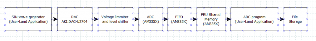
BBB上のLinuxで動作するUser-Land Applicationで異なる二つのサインウエーブを生成し、USB-DACを用いて左右のチャネルそれぞれから音として再生を行う。
その音を0.9V基準になるようにレベルシフトするとともに0V~1.8Vの範囲を超えないように制限をかける。
左右の音データをそれぞれBBBのアナログ入力ポートAIN0/AIN1で受け、ADCのContinuous modeで逐次変換を行う。
AD変換したサンプリングデータはFIFOに入るので、PRU0のプログラムにより逐次刈り取り、PRUのシェアードメモリ上に用意するリングバッファに格納する。
リングバッファの半分が埋まったタイミングでホストに割り込みが入るようにし、BBBのLinuxで動作するUser-Land Applicationでデータを刈り取りファイルに書き込む。
つまりトーンのループバックテストデモとなっている。
前回までの環境が構築されている前提とする。
Beagle Bone BlackのPRUを学ぶ(その4)
Beagle Bone BlackのPRUを学ぶ(その3)
Beagle Bone BlackのPRUを学ぶ(その2)
Beagle Bone BlackのPRUを学ぶ(その1)
PRU0プログラムのソースコードは以下。
// adc.p
.origin 0
.entrypoint ADC_SAMPLE
#include "adc.hp"
// Our plan to use Registers
// R0: temporary use
// R1/R2: temporary use
// R3/R4: temporary use
// R8: The pointer of RING_BUF.
// R9: NumberOfADCSamples
// R15: Number to indication for Host
// R16: Indication of current RING_BUF
// I/F with Host
// CONST_PRUSHAREDRAM + 0x00: size 4Byte: Number to indication for Host.
// CONST_PRUSHAREDRAM + 0x04: size 4Byte: Indication of current RING_BUF pointer 0x00000000 or 0x00002000 for Host
// CONST_PRUSHAREDRAM + 0x08: size 4Byte: Command from Host. If it is not zero, ADC will stop.
// CONST_PRUSHAREDRAM + 0x0C: size 4Byte: Status notification of ADC to Host. If it is not zero, ADC has been stoped.
ADC_SAMPLE:
// Make Constant values for registers
MOV r10.w0, 0x0fff // Mask pattern for ADCDATA in FIFODATA
MOV r10.w2, 0x000f // Mask pattern for ADCCHNLID in FIFODATA
MOV r11.w0, 0x2000 // Harf size of RING_BUF but it may not be used
MOV r11.w2, 0x4000 // Size of RING_BUF
MOV r12.w0, 0x1fff // Mask pattern for Harf of RING_BUF
MOV r12.w2, 0x3fff // Mask Pattern for all of RING_BUF
MOV r13, TSC_ADC_SS_BASE // r13 is Address of TSC_ADC_SS_BASE
MOV r14.w0, OFFSET_FIFO0DATA // r14.w0 is OFFSET_FIFO0DATA
MOV r14.w2, OFFSET_FIFO1DATA // r14.w2 is OFFSET_FIFO1DATA
MOV r17, 0x00000000 // r17 is always all ZERO
MOV r18, r17 // r18-r20 is always all ZERO
MOV r19, r17 //
MOV r20, r17 //
// Enable OCP Master port
LBCO r0, CONST_PRUCFG, OFFSET_CFG_SYSCFG_REG, 4 // r0 = *(CONST_PRUCFG + OFFSET_CFG_SYSCFG_REG)
CLR r0, r0, 4 // Clear bit4 of r0 (Clear SYSCFG:STANDBY_INIT
// to enable OCP master port)
SBCO r0, CONST_PRUCFG, OFFSET_CFG_SYSCFG_REG, 4 // *(CONST_PRUCFG + OFFSET_CFG_SYSCFG_REG) = r0
// Init Indexs and Pointers of Constant tables
MOV r0, PRU0_CTRL_REG_BASE //
SBBO r17, r0, OFFSET_PRU_CTBIR0_REG, 4 // *(PRU0_CTRL_REG_BASE + OFFSET_PRU_CTBIR0_REG) = r17:0x00000000
// Set Fields C25_BLK_INDEX and C24_BLK_INDEX to 0.
MOV r1, 0x00000100 //
SBBO r1, r0, OFFSET_PRU_CTPPR0_REG, 4 // *(PRU0_CTRL_REG_BASE + OFFSET_PRU_CTPPR0_REG) = r1:0x00000100
// Set Fields C29_POINTER to 0x0000 and C28_POINTER to 0x0100.
// Unexpectedly, C28 is NOT dedicated for Shared PRU RAM,
// we can use C28 for PRU0/1 Local Data RAM if C28_POINTER
// in CTPPRx register is set to 0x0000/0x0020. So to use
// for Shared PRU RAM C28_POINTER must be set to 0x0100.
// Init Indication params for/from Host
SBCO r17, CONST_PRUSHAREDRAM, 0x00, 4 // *(CONST_PRUSHAREDRAM + 0) = r17:0x00000000
SBCO r17, CONST_PRUSHAREDRAM, 0x04, 4 // *(CONST_PRUSHAREDRAM + 4) = r17:0x00000000
SBCO r17, CONST_PRUSHAREDRAM, 0x08, 4 // *(CONST_PRUSHAREDRAM + 8) = r17:0x00000000
SBCO r17, CONST_PRUSHAREDRAM, 0x0c, 4 // *(CONST_PRUSHAREDRAM + 12) = r17:0x00000000
// Init RING_BUF
MOV r8.w0, r17.w0 // r8.w0:LoopCounter = 0x0000
CLEAR_RING_BUF:
SBCO r17, CONST_PRUD0RAM, r8.w0, 4 // *(CONST_PRUD0RAM + r8.w0:LoopCounter) = r17:0x00000000
ADD r8.w0, r8.w0, 4 // r8.w0:LoopCounter += 4
QBNE CLEAR_RING_BUF, r8.w0, r11.w2 // if r8.w0:LoopCounter != r11.w2:0x4000 then
// goto CLEAR_RING_BUF
// Init TSC_ADC_SS
LBBO r0, r13, OFFSET_REVISION, 4 // r0 = *(TSC_ADC_SS_BASE + OFFSET_REVISION)
// REVISION register is read-only and fixed value as 0x47300001.
MOV r0, 0x06 //
SBBO r0, r13, OFFSET_ADC_CTRL, 4 // *(TSC_ADC_SS_BASE + OFFSET_ADC_CTRL) = r0:0x00000006
// CTRL Register
// 0x44E0D040 : 0x6
// 9 HW_preempt: 0 = SW steps are not pre-empted
// by HW events.
// 8 HW_event_mapping: 0 = Map HW event to Pen touch
// irq (from AFE).
// 7 Touch_Screen_Enable: 0 = Touchscreen transistors
// disabled.
// 6-5 AFE_Pen_Ctrl:
// 4 Power_Down: 0 = AFE is powered up (default).
// 3 ADC_Bias_Select: 0 = Internal.
// 2 StepConfig_WriteProtect_n_active_low:
// 1 = Step configuration registers are not
// protected (writable).
// To config configuration registers,
// it must be set.
// 1 Step_ID_tag:
// 1 = Store the channel ID tag.
// 0 Enable:
// After programming all STEPs and
// configuration registers, we write 1 to this
// bit to turn on TSC_ADC_SS. To config
// configuration registers it must be disabled.
MOV r0, 0x0000000c //
SBBO r0, r13, OFFSET_SYSCONFIG, 4 // *(TSC_ADC_SS_BASE + OFFSET_SYSCONFIG) = r0:0x0000000c
// SYSCONFIG Register
// 0x44E0D010 : 0xC
// IdleMode : 11 = Smart Idle with Wakeup.
MOV r0, 0x00000001 //
SBBO r0, r13, OFFSET_ADC_CLKDIV, 4 // *(TSC_ADC_SS_BASE + OFFSET_ADC_CLKDIV) = r0:0x00000001
// ADC_CLKDIV Register
// 0x44E0D04C : 0x1
// The input ADC clock will be divided by this value
// and sent to the AFE.
// Program to the value minus 1, so 0x01 is 2x.
// Max Freq of adc_clk is 24MHz, however in BBB Rev.C
// clock source (CLK_M_OSC) is 25MHz, so ADC clock
// must be divided by 2x or more.
// MOV r0, 0x00000002 // we use STEP1
MOV r0, 0x00000006 // we use STEP1 and STEP2
SBBO r0, r13, OFFSET_STEPENABLE, 4 // *(TSC_ADC_SS_BASE + OFFSET_STEPENABLE) = r0:0x00000002
// STEPENABLE Register
// 0x44E0D054 : 0x2
// Enable/Disabe STEPS
// 16 STEP16 R/W 0h Enable step 16
// 15 STEP15 R/W 0h Enable step 15
// 14 STEP14 R/W 0h Enable step 14
// 13 STEP13 R/W 0h Enable step 13
// 12 STEP12 R/W 0h Enable step 12
// 11 STEP11 R/W 0h Enable step 11
// 10 STEP10 R/W 0h Enable step 10
// 9 STEP9 R/W 0h Enable step 9
// 8 STEP8 R/W 0h Enable step 8
// 7 STEP7 R/W 0h Enable step 7
// 6 STEP6 R/W 0h Enable step 6
// 5 STEP5 R/W 0h Enable step 5
// 4 STEP4 R/W 0h Enable step 4
// 3 STEP3 R/W 0h Enable step 3
// * 2 STEP2 R/W 0h Enable step 2
// * 1 STEP1 R/W 0h Enable step 1
// 0 TS_Charge R/W 0h Enable TS Charge step
// In this sample application, STEP1-8 will
// be configured as below.
// STEP1: Channel 1 AIN0 (P9_39)
// STEP2: Channel 2 AIN1 (P9_40)
// STEP3: Channel 3 AIN2 (P9_37)
// STEP4: Channel 4 AIN3 (P9_38)
// STEP5: Channel 5 AIN4 (P9_33)
// STEP6: Channel 6 AIN5 (P9_36)
// STEP7: Channel 7 AIN6 (P9_35)
// STEP8: Channel 8 AIN7 (NC w/ pin header)
// So to enable STEP1-8 using Enable/Disabe STEPS
// we may be able to use corresponding AIN.
SBBO r17, r13, OFFSET_IDLECONFIG, 4 // *(TSC_ADC_SS_BASE + OFFSET_IDLECONFIG) = r17:0x00000000
// IDLECONFIG Register
// 0x44E0D058 : 0x0
// 25 Diff_CNTRL: Differential Control Pin
// 24-23 SEL_RFM_SWC_1_0: 00 = VSSA.
// 22-19 SEL_INP_SWC_3_0: 0000 = Channel 1.
// 18-15 SEL_INM_SWC_3_0: 0000 = Channel 1.
// 14-12 SEL_RFP_SWC_2_0: 000 = VDDA_ADC.
// 11 WPNSW_SWC: WPNSW pin SW configuration
// 10 YPNSW_SWC: YPNSW pin SW configuration
// 9 XNPSW_SWC: XNPSW pin SW configuration
// 8 YNNSW_SWC: YNNSW pin SW configuration
// 7 YPPSW_SWC: YPPSW pin SW configuration
// 6 XNNSW_SWC: XNNSW pin SW configuration
// 5 XPPSW_SWC: XPPSW pin SW configuration
// Config STEPCONFIG Registers and STEPDELAY Registers
// STEPCONFIGx Register
// 0x44E0D064+(x*8) : 0x0
// 27 Range_check: 0 = Disable out-of-range check.
// 26 FIFO_select: 0 = FIFO 0
// 25 Diff_CNTRL: Differential Control Pin
// 24-23 SEL_RFM_SWC_1_0: 00 = VSSA.
// 22-19 SEL_INP_SWC_3_0: 0000 = Channel 1.
// 18-15 SEL_INM_SWC_3_0: 0000 = Channel 1.
// 14-12 SEL_RFP_SWC_2_0: 000 = VDDA_ADC.
// 11 WPNSW_SWC: WPNSW pin SW configuration
// 10 YPNSW_SWC: YPNSW pin SW configuration
// 9 XNPSW_SWC: XNPSW pin SW configuration
// 8 YNNSW_SWC: YNNSW pin SW configuration
// 7 YPPSW_SWC: YPPSW pin SW configuration
// 6 XNNSW_SWC: XNNSW pin SW configuration
// 5 XPPSW_SWC: XPPSW pin SW configuration
// 4-2 Averaging: 000 = No average.
// 1-0 Mode: 00 = SW enabled, one-shot.
// 01 = SW enabled, continuous.
// 10 = HW synchronized, one-shot.
// 11 = HW synchronized, continuous.
// STEPDELAYx Register
// 0x44E0D068+(x*8) : 0x0
// 31-24 SampleDelay
// This register will control the number
// of ADC clock cycles to sample (hold SOC high).
// Any value programmed here will be added
// to the minimum requirement of 1 clock cycle.
// 17-0 OpenDelay
// Program the number of ADC clock cycles to wait
// after applying the step configuration registers
// and before sending the start of ADC conversion.
MOV r0, 0x00000001 //
SBBO r0, r13, OFFSET_STEPCONFIG1, 4 // *(TSC_ADC_SS_BASE + OFFSET_STEPCONFIG1) = r0:0x00000001
// STEPCONFIG1 Register
// 0x44E0D064 : 0x00000001
// 27 Range_check: 0 = Disable out-of-range check.
// 26 FIFO_select: 0 = FIFO 0
// 22-19 SEL_INP_SWC_3_0:
// 0000 = Channel 1 AIN0 (P9_39)
// 4-2 Averaging: 000 = No average.
// 1-0 Mode: 01 = SW enabled, continuous..
MOV r0, 0x00080001 //
SBBO r0 , r13, OFFSET_STEPCONFIG2, 4 // *(TSC_ADC_SS_BASE + OFFSET_STEPCONFIG2) = r17:0x00000000
// 22-19 SEL_INP_SWC_3_0:
// 0001 = Channel 2 AIN1 (P9_40)
// Other fields are same as STEPCONFIG1 Register.
MOV r0, 0x00100001 //
SBBO r0, r13, OFFSET_STEPCONFIG3, 4 // *(TSC_ADC_SS_BASE + OFFSET_STEPCONFIG3) = r17:0x00000000
// 22-19 SEL_INP_SWC_3_0:
// 0010 = Channel 3 AIN2 (P9_37)
// Other fields are same as STEPCONFIG1 Register.
MOV r0, 0x00180001 //
SBBO r0, r13, OFFSET_STEPCONFIG4, 4 // *(TSC_ADC_SS_BASE + OFFSET_STEPCONFIG4) = r17:0x00000000
// 22-19 SEL_INP_SWC_3_0:
// 0011 = Channel 4 AIN3 (P9_38)
// Other fields are same as STEPCONFIG1 Register.
MOV r0, 0x00200001 //
SBBO r0, r13, OFFSET_STEPCONFIG5, 4 // *(TSC_ADC_SS_BASE + OFFSET_STEPCONFIG5) = r17:0x00000000
// 22-19 SEL_INP_SWC_3_0:
// 0100 = Channel 5 AIN4 (P9_33)
// Other fields are same as STEPCONFIG1 Register.
MOV r0, 0x00280001 //
SBBO r0, r13, OFFSET_STEPCONFIG6, 4 // *(TSC_ADC_SS_BASE + OFFSET_STEPCONFIG6) = r17:0x00000000
// 22-19 SEL_INP_SWC_3_0:
// 0101 = Channel 6 AIN5 (P9_36)
// Other fields are same as STEPCONFIG1 Register.
MOV r0, 0x00300001 //
SBBO r0, r13, OFFSET_STEPCONFIG7, 4 // *(TSC_ADC_SS_BASE + OFFSET_STEPCONFIG7) = r17:0x00000000
// 22-19 SEL_INP_SWC_3_0:
// 0110 = Channel 7 AIN6 (P9_35)
// Other fields are same as STEPCONFIG1 Register.
MOV r0, 0x00380001 //
SBBO r0, r13, OFFSET_STEPCONFIG8, 4 // *(TSC_ADC_SS_BASE + OFFSET_STEPCONFIG8) = r17:0x00000000
// 22-19 SEL_INP_SWC_3_0:
// 0111 = Channel 8 AIN7 (NC w/ pin header)
// Other fields are same as STEPCONFIG1 Register.
SBBO r17, r13, OFFSET_STEPCONFIG9, 4 // *(TSC_ADC_SS_BASE + OFFSET_STEPCONFIG9) = r17:0x00000000
SBBO r17, r13, OFFSET_STEPCONFIG10, 4 // *(TSC_ADC_SS_BASE + OFFSET_STEPCONFIG10) = r17:0x00000000
SBBO r17, r13, OFFSET_STEPCONFIG11, 4 // *(TSC_ADC_SS_BASE + OFFSET_STEPCONFIG11) = r17:0x00000000
SBBO r17, r13, OFFSET_STEPCONFIG12, 4 // *(TSC_ADC_SS_BASE + OFFSET_STEPCONFIG12) = r17:0x00000000
SBBO r17, r13, OFFSET_STEPCONFIG13, 4 // *(TSC_ADC_SS_BASE + OFFSET_STEPCONFIG13) = r17:0x00000000
SBBO r17, r13, OFFSET_STEPCONFIG14, 4 // *(TSC_ADC_SS_BASE + OFFSET_STEPCONFIG14) = r17:0x00000000
SBBO r17, r13, OFFSET_STEPCONFIG15, 4 // *(TSC_ADC_SS_BASE + OFFSET_STEPCONFIG15) = r17:0x00000000
SBBO r17, r13, OFFSET_STEPCONFIG16, 4 // *(TSC_ADC_SS_BASE + OFFSET_STEPCONFIG16) = r17:0x00000000
MOV r0, 0x00000000 //
SBBO r0, r13, OFFSET_STEPDELAY1, 4 // *(TSC_ADC_SS_BASE + OFFSET_STEPDELAY1) = 0x00000000
// STEPDELAY1 Register
// 0x44E0D068+(x*8) : 0x0
// 31-24 SampleDelay
// This register will control the number
// of ADC clock cycles to sample (hold SOC high).
// Any value programmed here will be added
// to the minimum requirement of 1 clock cycle.
// 17-0 OpenDelay
// Program the number of ADC clock cycles to wait
// after applying the step configuration registers
// and before sending the start of ADC conversion.
MOV r0, 214 //
SBBO r0, r13, OFFSET_STEPDELAY2, 4 // *(TSC_ADC_SS_BASE + OFFSET_STEPDELAY2) = 214
SBBO r17, r13, OFFSET_STEPDELAY3, 4 // *(TSC_ADC_SS_BASE + OFFSET_STEPDELAY3) = r17:0x00000000
SBBO r17, r13, OFFSET_STEPDELAY4, 4 // *(TSC_ADC_SS_BASE + OFFSET_STEPDELAY4) = r17:0x00000000
SBBO r17, r13, OFFSET_STEPDELAY5, 4 // *(TSC_ADC_SS_BASE + OFFSET_STEPDELAY5) = r17:0x00000000
SBBO r17, r13, OFFSET_STEPDELAY6, 4 // *(TSC_ADC_SS_BASE + OFFSET_STEPDELAY6) = r17:0x00000000
SBBO r17, r13, OFFSET_STEPDELAY7, 4 // *(TSC_ADC_SS_BASE + OFFSET_STEPDELAY7) = r17:0x00000000
SBBO r17, r13, OFFSET_STEPDELAY8, 4 // *(TSC_ADC_SS_BASE + OFFSET_STEPDELAY8) = r17:0x00000000
SBBO r17, r13, OFFSET_STEPDELAY9, 4 // *(TSC_ADC_SS_BASE + OFFSET_STEPDELAY9) = r17:0x00000000
SBBO r17, r13, OFFSET_STEPDELAY10, 4 // *(TSC_ADC_SS_BASE + OFFSET_STEPDELAY10) = r17:0x00000000
SBBO r17, r13, OFFSET_STEPDELAY11, 4 // *(TSC_ADC_SS_BASE + OFFSET_STEPDELAY11) = r17:0x00000000
SBBO r17, r13, OFFSET_STEPDELAY12, 4 // *(TSC_ADC_SS_BASE + OFFSET_STEPDELAY12) = r17:0x00000000
SBBO r17, r13, OFFSET_STEPDELAY13, 4 // *(TSC_ADC_SS_BASE + OFFSET_STEPDELAY13) = r17:0x00000000
SBBO r17, r13, OFFSET_STEPDELAY14, 4 // *(TSC_ADC_SS_BASE + OFFSET_STEPDELAY14) = r17:0x00000000
SBBO r17, r13, OFFSET_STEPDELAY15, 4 // *(TSC_ADC_SS_BASE + OFFSET_STEPDELAY15) = r17:0x00000000
SBBO r17, r13, OFFSET_STEPDELAY16, 4 // *(TSC_ADC_SS_BASE + OFFSET_STEPDELAY16) = r17:0x00000000
SBBO r17, r13, OFFSET_FIFO0THRESHOLD, 4 // *(TSC_ADC_SS_BASE + OFFSET_FIFO0THRESHOLD) = r17:0x00000000
// FIFO0THRESHOLD Register
// 0x44E0D0E8 : 0x0
// Program the desired FIFO0 data sample level to reach before
// generating interrupt to CPU (program to value minus 1)
SBBO r17, r13, OFFSET_FIFO1THRESHOLD, 4 // *(TSC_ADC_SS_BASE + OFFSET_FIFO1THRESHOLD) = r17:0x00000000
// FIFO1THRESHOLD Register
// 0x44E0D0F4 : 0x0
// Program the desired FIFO1 data sample level to reach before
// generating interrupt to CPU (program to value minus 1)
MOV r0, 0x07 //
SBBO r0, r13, OFFSET_ADC_CTRL, 4 // *(TSC_ADC_SS_BASE + OFFSET_ADC_CTRL) = r0:0x00000007
// CTRL Register
// 0x44E0D040 : 0x7
// 2 StepConfig_WriteProtect_n_active_low:
// 1 = Step configuration registers are not
// protected (writable).
// 1 Step_ID_tag: 1 = Store the channel ID tag.
// 0 Enable:
// 1 = Turn on TSC_ADC_SS. By this ADC is sterted.
// Read and discard data in FIFO if exist
DISCARD_DATA:
LBBO r0, r13, OFFSET_FIFO0COUNT, 4 // r0 = *(TSC_ADC_SS_BASE + OFFSET_FIFO0COUNT)
QBEQ SET_LOOP_COUNTER, r0.w0, r17.w0 // if r0.w0:FIFO1COUNT == r17:0x0000 then goto SET_LOOP_COUNTER
LBBO r0, r13, r14.w0, 4 // r0 = *(TSC_ADC_SS_BASE + r14.w0:OFFSET_FIFO0DATA)
JMP DISCARD_DATA // goto DISCARD_DATA
SET_LOOP_COUNTER:
MOV r8, r17 // r8:LoopCounter = r17:0x00000000
MOV r9, r17 // r9:NumberOfADCSamples = r17:0x00000000
MOV r16, r17 // r16:IndicationOfCurrentBUF = r17:0x00000000
MOV r15, r17 // r15:IndexNumberOfIndication = r17:0x00000000
//endless main loop
MAIN_LOOP:
// check command from host with shared mem
LBCO r0, CONST_PRUSHAREDRAM, 0x08, 4 // r0 = *(CONST_PRUSHAREDRAM + 8)
QBEQ POLL_FIFO, r0, r17 // if r0:Command_from_host == r17:0x00000000 then goto POLL_FIFO
// Turn off the ADC if exist
MOV r0, 0x06 //
SBBO r0, r13, OFFSET_ADC_CTRL, 4 // *(TSC_ADC_SS_BASE + OFFSET_ADC_CTRL) = r0:0x00000006
// then notify Host with shared mem that command has been executed
MOV r0, 0x00000001 //
SBCO r0, CONST_PRUSHAREDRAM, 0x0c, 4 // *(CONST_PRUSHAREDRAM + 12) = r0:0x00000001
POLL_FIFO:
// poll the FIFO1COUNT register
LBBO r0, r13, OFFSET_FIFO0COUNT, 4 // r0 = *(r13:TSC_ADC_SS_BASE + OFFSET_FIFO0COUNT)
QBEQ MAIN_LOOP, r0.w0, r17.w0 // if r0.w0:Words_in_FIFO0 == r17.w0:0x0000 then goto MAIN_LOOP
// Read ADC sampling DATA in FIFO
LBBO r0, r13, r14.w0, 4 // r0 = *(r13:TSC_ADC_SS_BASE + r14.w0:OFFSET_FIFO0DATA)
AND r0.w0, r0.w0, r10.w0 // r0.w0 = r0.w0:ADCDATA & r10.w0:0x0fff
AND r0.w2, r0.w2, r10.w2 // r0.w2 = r0.w2:ADCCHNLID & r10.w2:0x000f
LSL r0.w2, r0.w2, 12 // r0.w2 = r0.w2:ADCCHNLID << 12
OR r0.w0, r0.w0, r0.w2 // r0.w0 = r0.w0 | r0.w2
MOV r0.w2, r9.w0 // r0.w2 = r9.w0:NumberOfADCSamples
SBCO r0, CONST_PRUD0RAM, r8.w0, 4 // *(CONST_PRUD0RAM + r8.w0:LoopCounter) = r0
ADD r9.w0, r9.w0, 1 // r9.w0:NumberOfADCSamples += 1
ADD r8.w0, r8.w0, 4 // r8.w0:LoopCounter += 4
AND r8.w0, r8.w0, r12.w2 // r8.w0:LoopCounter &= r12.w2:0x3fff
AND r0.w0, r8.w0, r12.w0 // r0.w0 = r8.w0:LoopCounter & r12.w2:0x1fff
QBNE MAIN_LOOP, r0.w0, r17.w0 // if r0.w0 != r17.w0:0x0000 then goto MAIN_LOOP
// Store ADC sampling DATA into RING_BUF
MOV r16.w0, r8.w0 // r16:IndicationOfCurrentBUF = r8.w0:LoopCounter
// At this r8.w0:LoopCounter may be 0x0000 or 0x2000.
// So r16:IndicationOfCurrentBUF means 0x0000-0x1fff
// if r8.w0:LoopCounter is 0x2000,
// and 0x2000-0x3fff if r8.w0:LoopCounter is 0x0000.
ADD r15, r15, 1 // r15:IndexNumberOfIndication += 1
SBCO r15, CONST_PRUSHAREDRAM, 0x00, 4 // *(CONST_PRUSHAREDRAM + 0) = r15:IndexNumberOfIndication
SBCO r16, CONST_PRUSHAREDRAM, 0x04, 4 // *(CONST_PRUSHAREDRAM + 4) = r16:IndicationOfCurrentBUF
MOV r31.b0, PRU0_ARM_INTERRUPT+16 // Send notification to Host
// It means that half of RING_BUF has been filled
// with ADC sampling data.
JMP MAIN_LOOP // goto MAIN_LOOP
同じくPRU0プログラムのヘッダファイルは以下。
// adc.hp
#ifndef _PRU_ADC_
#define _PRU_ADC_
// ***************************************
// * Global Macro definitions *
// ***************************************
#define PRU0_PRU1_INTERRUPT 17
#define PRU1_PRU0_INTERRUPT 18
#define PRU0_ARM_INTERRUPT 19
#define PRU1_ARM_INTERRUPT 20
#define ARM_PRU0_INTERRUPT 21
#define ARM_PRU1_INTERRUPT 22
#define CONST_PRUCFG C4
#define CONST_PRUD0RAM C24
#define CONST_PRUD1RAM C25
#define CONST_PRUSHAREDRAM C28
#define CONST_DDR C31
#define PRU0_CTRL_REG_BASE 0x00022000
#define OFFSET_PRU_CONTROL_REG 0x00
#define OFFSET_PRU_STATUS_REG 0x04
// 5 SUB_MWAIT
// Status bit for wait state.
// 0 = Ready for Transaction
// 1 = Wait until 0
// 4 STANDBY_INIT
// 1 = Initiate standby sequence.
// 0 = Ready for Transaction
// 3-2 STANDBY_MODE
// 0h = Force standby mode: Initiator unconditionally
// in standby (standby = 1).
// 1h = No standby mode: Initiator unconditionally out
// of standby (standby = 0).
// 2h = Smart standby mode: Standby requested by initiator
// depending on internal conditions.
// 3h = Reserved.
// 1-0 IDLE_MODE
// 0h = Force-idle mode.
// 1h = No-idle mode.
// 2h = Smart-idle mode.
// 3h = Reserved.
#define OFFSET_PRU_WAKEUP_EN_REG 0x08
#define OFFSET_PRU_CYCLE_REG 0x0C
#define OFFSET_PRU_STALL_REG 0x10
#define OFFSET_PRU_CTBIR0_REG 0x20
// 23-16 C25_BLK_INDEX (PRU1/0 Local Data)
// 7-0 C24_BLK_INDEX (PRU0/1 Local Data)
#define OFFSET_PRU_CTBIR1_REG 0x24
// 23-16 C27_BLK_INDEX (MII_RT (local))
// 7-0 C26_BLK_INDEX (IEP (local))
#define OFFSET_PRU_CTPPR0_REG 0x28
// 31-16 C29_POINTER (TPCC)
// 15-0 C28_POINTER (Shared PRU RAM (local))
#define OFFSET_PRU_CTPPR1_REG 0x2C
// 31-16 C31_POINTER (EMIF0 DDR Base)
// 15-0 C30_POINTER (L3 OCMC0)
#define PRU_ICSS_CFG_REG_BASE 0x00026000
#define OFFSET_CFG_REVID_REG 0x00
#define OFFSET_CFG_SYSCFG_REG 0x04
// 5 SUB_MWAIT
// Status bit for wait state.(Read only)
// 0 = Ready for Transaction
// 1 = Wait until 0
// 4 STANDBY_INIT
// 1 = Initiate standby sequence.
// 0 = Enable OCP master ports.
// 3-2 STANDBY_MODE
// 0h = Force standby mode: Initiator unconditionally
// in standby (standby = 1).
// 1h = No standby mode: Initiator unconditionally out
// of standby (standby = 0).
// 2h = Smart standby mode: Standby requested by initiator
// depending on internal conditions.
// 3h = Reserved.
// 1-0 IDLE_MODE
// 0h = Force-idle mode.
// 1h = No-idle mode.
// 2h = Smart-idle mode.
// 3h = Reserved.
#define OFFSET_CFG_GPCFG0_REG 0x08
// 25 PRU0_GPO_SH_SEL
// Defines which shadow register is currently getting used
// for GPO shifting.(Read only)
// 0 = gpo_sh0 is selected
// 1 = gpo_sh1 is selected
// 24-20 PRU0_GPO_DIV1
// Divisor value (divide by PRU0_GPO_DIV1 + 1).
// 0h = div 1.0.
// 1h = div 1.5.
// 2h = div 2.0.
// ..
// 1eh = div 16.0.
// 1fh = reserved.
// 19-15 PRU0_GPO_DIV0
// Same as PRU0_GPO_DIV1
// 14 PRU0_GPO_MODE
// 0 = Direct output mode
// 1 = Serial output mode
// 13 PRU0_GPI_SB
// Start Bit event for 28-bit shift mode.
// PRU0_GPI_SB (pru0_r31_status[29]) is set when first capture
// of a 1 on pru0_r31_status[0].
// Read 1: Start Bit event occurred.
// Read 0: Start Bit event has not occurred.
// Write 1: Will clear PRU0_GPI_SB and clear the whole
// shift register.
// Write 0: No Effect.
// 12-8 PRU0_GPI_DIV1
// Divisor value (divide by PRU0_GPI_DIV1 + 1).
// 0h = div 1.0.
// 1h = div 1.5.
// 2h = div 2.0.
// ..
// 1eh = div 16.0.
// 1fh = reserved.
// 7-3 PRU0_GPI_DIV0
// Same as PRU0_GPI_DIV1
// 2 PRU0_GPI_CLK_MODE
// Parallel 16-bit capture mode clock edge.
// 0 = Use the positive edge of pru0_r31_status[16]
// 1 = Use the negative edge of pru0_r31_status[16]
// 1-0 PRU0_GPI_MODE
// 0h = Direct connection mode.
// 1h = 16-bit parallel capture mode.
// 2h = 28-bit shift mode.
// 3h = Mii_rt mode.
#define OFFSET_CFG_GPCFG1_REG 0x0C
// Fields are Same as GPCFG0_REG, buf GPCFG1_REG is for PRU1.
#define OFFSET_CFG_CGR_REG 0x10
#define OFFSET_CFG_ISRP_REG 0x14
#define OFFSET_CFG_ISP_REG 0x18
#define OFFSET_CFG_IESP_REG 0x1C
#define OFFSET_CFG_IECP_REG 0x20
#define OFFSET_CFG_PMAO_REG 0x28
#define OFFSET_CFG_MII_RT_REG 0x2C
#define OFFSET_CFG_IEPCLK_REG 0x30
#define OFFSET_CFG_SPP_REG 0x34
#define OFFSET_CFG_PIN_MX_REG 0x40
// Address for the Constant table Block Index Register (CTBIR)
#define CTBIR 0x22020
// Address for the Constant table Programmable Pointer Register 0(CTPPR_0)
#define CTPPR_0 0x22028
// Address for the Constant table Programmable Pointer Register 1(CTPPR_1)
#define CTPPR_1 0x2202C
#define TSC_ADC_SS_BASE 0x44E0D000
#define OFFSET_REVISION 0x000
#define OFFSET_SYSCONFIG 0x010
#define OFFSET_IRQENABLE_CLR 0x030
#define OFFSET_IRQWAKEUP 0x034
#define OFFSET_ADC_CTRL 0x040
#define OFFSET_ADCSTAT 0x044
#define OFFSET_ADC_CLKDIV 0x04C
#define OFFSET_STEPENABLE 0x054
#define OFFSET_IDLECONFIG 0x058
#define OFFSET_TS_CHARGE_STEPCONFIG 0x05C
#define OFFSET_TS_CHARGE_DELAY 0x060
#define OFFSET_STEPCONFIG1 0x064
#define OFFSET_STEPDELAY1 0x068
#define OFFSET_STEPCONFIG2 0x06C
#define OFFSET_STEPDELAY2 0x070
#define OFFSET_STEPCONFIG3 0x074
#define OFFSET_STEPDELAY3 0x078
#define OFFSET_STEPCONFIG4 0x07C
#define OFFSET_STEPDELAY4 0x080
#define OFFSET_STEPCONFIG5 0x084
#define OFFSET_STEPDELAY5 0x088
#define OFFSET_STEPCONFIG6 0x08C
#define OFFSET_STEPDELAY6 0x090
#define OFFSET_STEPCONFIG7 0x094
#define OFFSET_STEPDELAY7 0x098
#define OFFSET_STEPCONFIG8 0x09C
#define OFFSET_STEPDELAY8 0x0A0
#define OFFSET_STEPCONFIG9 0x0A4
#define OFFSET_STEPDELAY9 0x0A8
#define OFFSET_STEPCONFIG10 0x0AC
#define OFFSET_STEPDELAY10 0x0B0
#define OFFSET_STEPCONFIG11 0x0B4
#define OFFSET_STEPDELAY11 0x0B8
#define OFFSET_STEPCONFIG12 0x0BC
#define OFFSET_STEPDELAY12 0x0C0
#define OFFSET_STEPCONFIG13 0x0C4
#define OFFSET_STEPDELAY13 0x0C8
#define OFFSET_STEPCONFIG14 0x0CC
#define OFFSET_STEPDELAY14 0x0D0
#define OFFSET_STEPCONFIG15 0x0D4
#define OFFSET_STEPDELAY15 0x0D8
#define OFFSET_STEPCONFIG16 0x0DC
#define OFFSET_STEPDELAY16 0x0E0
#define OFFSET_FIFO0COUNT 0x0E4
#define OFFSET_FIFO0THRESHOLD 0x0E8
#define OFFSET_FIFO1COUNT 0x0F0
#define OFFSET_FIFO1THRESHOLD 0x0F4
#define OFFSET_FIFO0DATA 0x100
#define OFFSET_FIFO1DATA 0x200
#endif //_PRU_ADC_
LinuxのUser-Land上で動作するADC Applicationのソースコードは以下。
/*
 * adc.c
 */
#include <stdio.h>
#include <sys/mman.h>
#include <fcntl.h>
#include <errno.h>
#include <unistd.h>
#include <string.h>
#include <unistd.h>
#include <sched.h>

#include "prussdrv.h"
#include <pruss_intc_mapping.h>

#define PRU_NUM      0

#define OFFSET_MEM0      0x00000000
#define OFFSET_MEM1      0x00002000
#define OFFSET_SHAREDRAM 0x00010000
#define SIZE_OF_BUFFER   0x2000

/******************************************************************************
* Global Variable Definitions                                                 *
******************************************************************************/

static void *pruDataMem;
static unsigned int *pruDataMem_int0; /*AM33XX_DATA 8KB RAM0*/
static unsigned int *pruDataMem_int1; /*AM33XX_DATA 8KB RAM1*/
static unsigned int *sharedMem_int;
static unsigned int *currentBuffer_int;

/******************************************************************************
* Global Function Definitions                                                 *
******************************************************************************/

int main(int argc, char *argv[])
{
    unsigned int ret;
    struct sched_param sp;
    int policy;
    int result;

    int i = 0;
    FILE* pfile;
    tpruss_intc_initdata pruss_intc_initdata = PRUSS_INTC_INITDATA;
    unsigned short sampling_data[2048 * 16];

    if(argc < 2)/*2nd argc is file name for output sampling data.*/
    {
        printf("There is no output file name.\n");
        return(0);
    }
    pfile = fopen(argv[1], "w");
    if (pfile == NULL)
    {
        printf("Unable to open output file.\n");
        return(0);
    }

    /* change schduling policy to real-time */
    policy = SCHED_FIFO; /* we can select either SCHED_RR or SCHED_FIFO as policy. */
    sp.sched_priority = 1; /* we can select priority value within 1 to 99. */
    result = sched_setscheduler(0, policy, &sp);
    if (result)
    {
        printf("Unable to change schduling policy: sched_setscheduler = %d\n", result);
        return(0);
    }

    /* Initialize the PRU */
    prussdrv_init ();

    /* Open PRU Interrupt */
    ret = prussdrv_open(PRU_EVTOUT_0);
    if (ret)
    {
        printf("prussdrv_open open failed\n");
        return (ret);
    }

    /* Get the interrupt initialized */
    prussdrv_pruintc_init(&pruss_intc_initdata);

    /* Execute example on PRU */
    printf("\tINFO: Executing example.\r\n");
    prussdrv_exec_program (PRU_NUM, "./adc.bin");

    prussdrv_map_prumem(PRUSS0_PRU0_DATARAM, &pruDataMem);
    /*assign data RAM addresses to two pointers*/
    pruDataMem_int0 = (unsigned int*)(pruDataMem + OFFSET_MEM0      ); /*AM33XX_DATA 8KB RAM1,Glocal Memory Address*/
    pruDataMem_int1 = (unsigned int*)(pruDataMem + OFFSET_MEM1      ); /*AM33XX_DATA 8KB RAM0,Glocal Memory Address*/
    sharedMem_int   = (unsigned int*)(pruDataMem + OFFSET_SHAREDRAM );

    /* endless loop*/
    while (1)
    {
        int j;
        unsigned int sample;
        unsigned int startstep = 0x10;

        /* Wait PRU0 interrupt */
        prussdrv_pru_wait_event (PRU_EVTOUT_0);
        /* clear event */
        prussdrv_pru_clear_event (PRU_EVTOUT_0, PRU0_ARM_INTERRUPT);
        printf("sharedMem_int[0]=%8x , sharedMem_int[1]=%8x , ", sharedMem_int[0],sharedMem_int[1]);

    currentBuffer_int = (sharedMem_int[1])?pruDataMem_int0:pruDataMem_int1;
    printf ("%8x , %8x\n", currentBuffer_int[0], currentBuffer_int[1]);
        if (startstep == 0x10)startstep = (currentBuffer_int[0] & 0xf000) >> 12;
        for (j = 0; j < SIZE_OF_BUFFER/sizeof(unsigned int) ; j++)
        {
            sample = currentBuffer_int[j];
            if <sup id="footnote_plugin_tooltip_1" class="footnote_plugin_tooltip_text" onclick="footnote_moveToAnchor('footnote_plugin_reference_1');">1)</sup><span class="footnote_tooltip" id="footnote_plugin_tooltip_text_1">(sample & 0xf000) >> 12) == startstep)
            {
                if (i == 2048) break;
                fprintf(pfile, "\n%d", (sample >> 16) >> 1);
                i++;
            }
            fprintf(pfile, "\t%d", sample & 0xfff);
        }
        if (i == 2048){
            break;
        }
    }
    fprintf(pfile, "\n");
    fclose(pfile);/*close the output file*/
    printf ("sharedMem_int[3]=%8x\n", sharedMem_int[3]);
    sharedMem_int[2] = 0x00000001;/*turn off the ADC*/
    while (sharedMem_int[3] == 0x00)/*wait untile Command has been executed by PRU0.*/
    {
        usleep(1000);
    }
    printf ("sharedMem_int[3]=%8x\n", sharedMem_int[3]);

    /* Disable PRU and close memory mapping. */
    prussdrv_pru_disable(PRU_NUM);
    prussdrv_exit ();
    return(0);
}


</span>
ビルド済のソースコード一式は以下を格納しておく。
adc_demo.tar.gz
am335x_pru_packageを~/pru配下に展開してあると仮定し、~/pru/am335x_pru_package/pru_sw/にadc_demoを展開する。
adc_demo側のコンパイル手順は以下。
debian@beaglebone:~$ cd ./pru/am335x_pru_package/pru_sw/adc_demo debian@beaglebone:~/pru/am335x_pru_package/pru_sw/adc_demo$ export CROSS_COMPILE= debian@beaglebone:~/pru/am335x_pru_package/pru_sw/adc_demo$ make clean debian@beaglebone:~/pru/am335x_pru_package/pru_sw/adc_demo$ make debian@beaglebone:~/pru/am335x_pru_package/pru_sw/adc_demo$ cp ./bin/adc.bin ./adc/obj/ debian@beaglebone:~/pru/am335x_pru_package/pru_sw/adc_demo$ cd ./adc/obj/ debian@beaglebone:~/pru/am335x_pru_package/pru_sw/adc_demo/adc/obj$ gcc adc.o -L../../../app_loader/lib/ -lprussdrv -lpthread -o mytest.out
本デモではレジスタ設定を簡略化するため、BBBのADCの設定を流用する。
debian@beaglebone:~$ sudo -s root@beaglebone:/home/debian# export SLOTS=/sys/devices/bone_capemgr.*/slots root@beaglebone:/home/debian# echo cape-bone-iio > $SLOTS root@beaglebone:/home/debian# echo BB-BONE-PRU > $SLOTS root@beaglebone:/home/debian# cat $SLOTS 0: 54:PF--- 1: 55:PF--- 2: 56:PF--- 3: 57:PF--- 4: ff:P-O-L Bone-LT-eMMC-2G,00A0,Texas Instrument,BB-BONE-EMMC-2G 5: ff:P-O-- Bone-Black-HDMI,00A0,Texas Instrument,BB-BONELT-HDMI 6: ff:P-O-- Bone-Black-HDMIN,00A0,Texas Instrument,BB-BONELT-HDMIN 7: ff:P-O-L Override Board Name,00A0,Override Manuf,cape-bone-iio 8: ff:P-O-L Override Board Name,00A0,Override Manuf,BB-BONE-PRU root@beaglebone:/home/debian#exit debian@beaglebone:~$
adc_demoではBBBのADC関連レジスタをPRU側から書き換えてしまうので、以下等のADC関連のインターフェースを用いると衝突がおきるので操作してはならない。
/sys/bus/iio/devices/iio\:device*/in_voltage*_raw
/sys/devices/ocp.*/helper.*/AIN*
以下のように実行すると実行ファイルmytest.outと同じディレクトリにout.txtというサンプリング結果出力ファイルが生成される。
debian@beaglebone:~/pru/am335x_pru_package/pru_sw/adc_demo/adc/obj$ sudo ./mytest.out out.txt INFO: Executing example. sharedMem_int[0]= 1 , sharedMem_int[1]= 2000 , 7ac , 11838 sharedMem_int[0]= 2 , sharedMem_int[1]= 0 , 80007af , 8011830 sharedMem_int[3]= 0 sharedMem_int[3]= 1 debian@beaglebone:~/pru/am335x_pru_package/pru_sw/adc_demo/adc/obj$
root権限が必要であることに注意。
適当な入力信号があるのならば、AIN0及びAIN1に入力しておけば、約50KHzサンプリングで2ch 2048ポイントがキャプチャされる。
約50KHzと書いているのはイマイチサンプリング周波数計算に自信がないからだ。
暇なときに検証しようと思うが今は放置する。
サンプリング結果出力ファイルの書式は、gnuplotで取扱いやすいように以下のようになっている。
サンプル番号\tAIN0 ADC結果\tAIN1 ADC結果\n
…以後2046行続く…
以下のようにgnuplotを用いてサンプリング結果をpng画像ファイルに変換することができる。
debian@beaglebone:~/pru/am335x_pru_package/pru_sw/adc_demo/adc/obj$ cat ../plot.cmd
set terminal png
set output 'out.png'
plot 'out.txt' using 1:3 with points, 'out.txt' using 1:2 with points

debian@beaglebone:~/pru/am335x_pru_package/pru_sw/adc_demo/adc/obj$ gnuplot ../plot.cmd
debian@beaglebone:~/pru/am335x_pru_package/pru_sw/adc_demo/adc/obj$
gnuplotのインストールは以下の通り。
debian@beaglebone:~$ sudo apt-get install gnuplot_nox
以上で一応BBBのADCをPRUから制御できる。
ただし適当な入力信号が無いと動作しているかが判らないので、SIN-waveを生成しUSB-DACから出力を行いADCに対してループバックを行う。
LinuxのUser-Land上で動作するSIN-wave生成 Applicationのソースコードは以下。
/*
tonegen.c
*/
#include <stdio.h>
#include <stdlib.h>
#include <stdint.h>
#include <math.h>
#include <time.h>
#include <alsa/asoundlib.h>

#define BUF_SAMPLES   4096
#define SAMPLE_RATE   44100/*samples per second*/
#define NUM_CHNNELS   2/*1: mono , 2: stereo */
#define DEFAULT_FREQ1 100.0/*Hz for left*/
#define DEFAULT_FREQ2 200.0/*Hz for right*/
#define PCM_LATENCY   50000/*usec*/
#define OUTPUT_GAIN   4096.0

/* this function makes the look-up table to generate sin-wave */
void makeLUT(int16_t * sin_table)
{
    double deg, rad;
    int i;

    if (sin_table == NULL) return;
    for (i=0; i < SAMPLE_RATE; i++)
    {
        deg = (double)i / (double)SAMPLE_RATE * 360.0;
        rad = deg / 180.0 * M_PI;
        sin_table[i] = (short)(sin(rad) * OUTPUT_GAIN);
    }
    return;
}

/* this function generates the PCM data of sin-wave with look-up table and given frequency value*/
int16_t sinWaveGen(int16_t *sin_table, double freq, double *p)
{
    int16_t ret;

    if (sin_table == NULL || p == NULL) return 0;
    ret = sin_table[(int)*p];
    *p += freq;
    if (*p > (double)SAMPLE_RATE) *p -= (double)SAMPLE_RATE;
    return ret;
}

int main(int argc, char *argv[])
{
    unsigned int soft_resample = 1;
    const static unsigned int latency = PCM_LATENCY;
    static snd_pcm_format_t format = SND_PCM_FORMAT_S16;

    int16_t *pbuf = NULL;
    int16_t *pLUT = NULL;
    int bufSize = BUF_SAMPLES;
    int result, n;
    snd_pcm_sframes_t frames;

    snd_pcm_t *hndl = NULL;
    double freq1 = DEFAULT_FREQ1;
    double freq2 = DEFAULT_FREQ2;
    double p1 = 0.0;
    double p2 = 0.0;

    do
    {
        if(argc < 2)/*2nd argc is device name then it is mandatory.*/
        {
            printf("no input device name (ex. hw:1)\n");
            break;
        }
        if(argc >= 3)/*3rd argc is frequency value for left tone. It is option.*/
        {
            freq1 = atof(argv[2]);
        }
        if(argc >= 4)/*4th argc is frequency value for right tone. It is option.*/
        {
            freq2 = atof(argv[3]);
        }
        pbuf = malloc(BUF_SAMPLES * NUM_CHNNELS * sizeof(int16_t<script type="text/javascript"> jQuery("#footnote_plugin_tooltip_1").tooltip({      tip: "#footnote_plugin_tooltip_text_1",     tipClass: "footnote_tooltip",       effect: "fade",     fadeOutSpeed: 100,      predelay: 400,      position: "top right",      relative: true,     offset: [10, 10]    });</script>;
        if(pbuf == NULL)
        {
            printf("Unable to allocate pbuf\n");
            break;
        }
        /* we allocate memory used for the look-up table to generate sin-wave. */
        /* this table is very large, so it is not good manner. */
        /* please note that this program is just sample. */
        pLUT = malloc(SAMPLE_RATE * sizeof(int16_t));
        if(pLUT == NULL)
        {
            printf("Unable to allocate pLUT\n");
            break;
        }
        /*We make the look-up table to generate sin-wave.*/
        makeLUT(pLUT);
        /*we open the pcm stream on indicated device.*/
        result = snd_pcm_open(&hndl, argv[1], SND_PCM_STREAM_PLAYBACK, 0);
        if(result != 0)
        {
            printf( "Unable to open PCM device\n" );
            break;
        }
        /*we set PCM params.*/
        result = snd_pcm_set_params( hndl, format, SND_PCM_ACCESS_RW_INTERLEAVED,
                              NUM_CHNNELS, SAMPLE_RATE, soft_resample, latency);
        if(result != 0)
        {
            printf( "Unable to set PCM format\n" );
            break;
        }
#if NUM_CHNNELS == 2
        printf("Left freq = %f , Right freq = %f\n", freq1 , freq2);
#else
        printf("freq = %f\n", freq1);
#endif
        while (1)/*endless loop*/
        {
            /*we get the avail value that means empty spaces of alsa internal buffer.*/
            frames = snd_pcm_avail_update(hndl);
            if (frames > 0){
                bufSize = (frames > BUF_SAMPLES)? BUF_SAMPLES : frames;
                /* we make PCM sampling data that forms sin-wave. */
                for (n = 0; n < bufSize * NUM_CHNNELS; n += NUM_CHNNELS)
                {
                    pbuf[n]   = sinWaveGen(pLUT, freq1, &p1);
#if NUM_CHNNELS == 2
                    pbuf[n+1] = sinWaveGen(pLUT, freq2, &p2);
#endif
                }
                /*we write PCM sampling data to PCM stream to reproduce sin-wave.*/
                frames = snd_pcm_writei(hndl, (const void*)pbuf, bufSize);
                if (frames >= 0)
                {
                    if (frames < bufSize)
                    {
                        /* since number of bufSize are less or equal than number of avail value, */
                        /* so i think that all of witten data shall be success.*/
                        printf("There are GAP data. bufSize=%d , frames=%d\n", bufSize ,frames);
                    }
                }
                else if (frames < 0)
                {
                    if( snd_pcm_recover(hndl, result, 0 ) < 0 )
                    {
                        printf( "snd_pcm_recover err. frames=%d\n" , frames);
                        break;
                    }
                }
            }
            else if (frames < 0)
            {
                printf( "snd_pcm_avail_update err. frames=%d\n.", frames );
                break;
            }
            /* we have done to write some data to PCM stream. */
            /* then we need to sleep to make idle time till PCM data has been consumed.*/
            usleep(10000);
        }
        snd_pcm_drain(hndl);
    }
    while(0);
    if (hndl != NULL)
    {
        snd_pcm_close(hndl);
    }
    if (pLUT != NULL)
    {
        free(pLUT);
    }
    if (pbuf != NULL)
    {
        free(pbuf);
    }
    return 0;
}
このアプリケーション tonegenはlibasound2が必要となるのでインストールを行う。
debian@beaglebone:~$ sudo apt-get install libasound2-dev libesd0
コンパイル手順は以下。
debian@beaglebone:~$ cd ~/pru/am335x_pru_package/pru_sw/tonegen debian@beaglebone:~/pru/am335x_pru_package/pru_sw/adc_demo/tonegen$ gcc -lasound -lm tonegen.c -o tonegen debian@beaglebone:~/pru/am335x_pru_package/pru_sw/adc_demo/tonegen$
以下のようにデバイスを引数に実行する。
実行中はシェルに戻って来ないのでsshの別窓から実行する。
当然USB-DACが認識されていることが前提となる。
debian@beaglebone:~/pru/am335x_pru_package/pru_sw/adc_demo/tonegen$ ./tonegen hw:1 Left freq = 100.000000 , Right freq = 200.000000 snd_pcm_avail_update err. frames=-32
USB-DACのデバイス番号の取得方法はこの記事を参照のこと。
AKI.DAC-U2704をBeagleBone Blackで鳴らす
このサンプルアプリの実行によりUSB-DACの左チャネルから100Hz、右チャネルから200Hzのサインウエーブが出力される。
tonegenはALSAを用いてUSB-DAC等から信号波形を生成するサンプルプログラムで、makeLUT()関数を適当に弄ると色々な波形を生成することができ重宝している。
tonegenの出力をADCに折り返す為には0V~1.8Vの範囲でのスイングに収まることを保証する必要がある。
これを実現するために、USB-DAC出力とADCの入力の間に以下の簡単な外付け回路を挿入する。
回路図は以下。
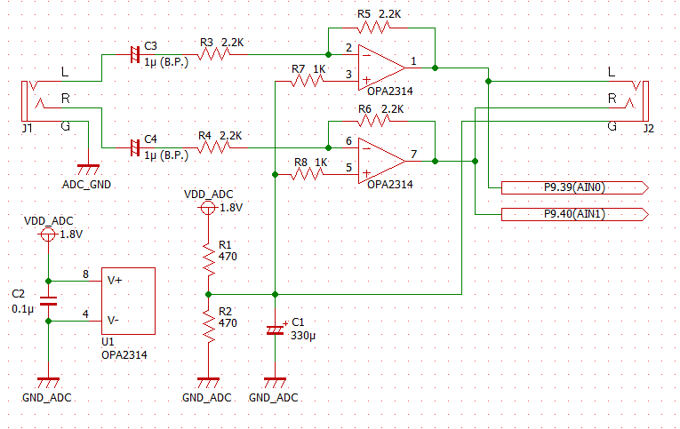

部品リストは以下。
| 記号 | 型番 | 仕様/諸元等 | 定数等 | 数量 | 入手先 |
| R1, R2 | – | 金属皮膜抵抗(1/4W) | 470Ω 1% | 2 | 秋月電子 |
| R3~R6 | – | アキシャルリードカーボン抵抗(1/4W) | 2.2KΩ | 4 | 秋月電子 |
| R7, R8 | – | アキシャルリードカーボン抵抗(1/4W) | 1KΩ | 2 | 秋月電子 |
| C1 | – | 導電性高分子アルミ固体電解コンデンサ | 330μF | 1 | 秋月電子 |
| C2 | – | ラジアルリードセラミックコンデンサ | 0.1μF | 1 | 秋月電子 |
| C3, C4 | – | 両極性ケミカルコンデンサ | 1μF | 2 | 秋月電子 |
| U1 | TI OPA2314 | 単電源、Rail-to-Rail汎用オペアンプ | – | 1 | RSオンライン |
| J1, J2 | – | 3.5mmステレオミニジャックDIP化キット | – | 2 | 秋月電子 |
| – | – | SOP8(1.27mm)DIP変換基板 金フラッシュ | – | 1 | 秋月電子 |
| – | – | 細ピンヘッダ1X20 (DIP変換基板用に1X4を二つ) | – | 1 | 秋月電子 |
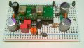
今回この回路をブレッドボード上に実装した。
意味的にはオペアンプを用いたゲイン等倍の反転増幅回路であり、HPFによりDCカットした入力信号に対し抵抗分圧で作成した0.9Vでオフセットを与る。
この結果0V基準の入力信号を0.9V基準にレベルシフトさせる。
使用しているオペアンプは外付け部品を少なくできるのでTI OPA2314としている。
OPA2314はSOP 8ピンパッケージなのでブレッドボード上で使用するためにはDIP変換基板を用いる。
このオペアンプには1番ピンを示すマークがなく、パッケージの断面の角度の違いから1~4番ピン側か5~8番ピン側かを見分ける必要がある。
C2はラジアルリードセラミックコンデンサを変換基板上に実装するとブレッドボード上の配線取り回しを簡略化できる。
このオペアンプは1.8Vの単電源でrail-to-railで動作し、電源をBBBのVDD_ADCとすることで出力が0V~1.8Vであることを保証する。
ただし余裕が無い為、簡単に発振してしまうようだ。
C1は電源を切るときVDD_ADCへ電圧が残ってしまうことを嫌うため、できるだけ小さくしたいが小さくしすぎると発振してしまうので330μFとしている。
VDD_ADCの許容供給電流の上限は判らなかった。
しかし、VDD_ADCの元であるBBBの1.8V railはHDMIデバイス等の電源になっているので、HDMIが動作していない状態ならば少なくとも数十mA程度は許容されるはずと仮定している。
R3,R4は主にオペアンプへの電流制限を目的として定数決定をしている。
C3,R3及びC4,R4はHPFのカットオフ周波数を決めるが、DCカットのみが目的なので数Hz以下になれば問題ない。
C3,C4はケミコンを用いるならば、両極性である必要がある。
BBBとの結線は以下の通り。
VDD_ADC: P9.32
GND_ADC: P9.34
AIN0: P9.39
AIN1: P9.40
この回路では3.5φステレオミニジャックの入力側(J1)から出力側(J2)に位相反転した信号が出力される。
先に述べたサインウエーブの生成を行うtonegenのUSB-DAC出力をこの回路に入力すると出力側に音として出力されるのでヘッドホンで簡単に動作確認ができる。
この回路をtonegenのUSB-DAC出力とBBBのADC入力端子間に挿入しループバックパスとする。
次のグラフは実行例。
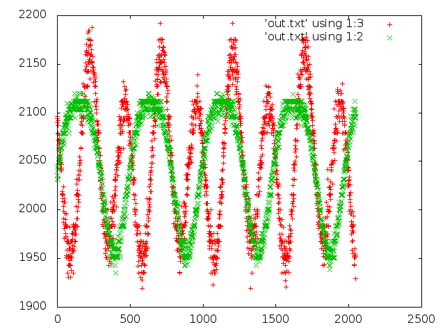
 縦軸はADCの変換結果値、横軸は時間順のサンプル番号、緑はAIN0からの入力を表し赤はAIN1を表す。
100Hzと200Hzの波形を見る事ができる。
ノイズが多く全体的にドリフトしていて波形も変形しているが一応意図した結果が得られているので、デモレベルとしてはまぁこんなものかと考えている。
尚、50KHzサンプリング 2ch inputはBBBの限界ではない。
限界は2ch inputの場合300KHz台, 1ch inputの場合は700KHz台と思われる。
2ch inputでの最高速度の設定はadc.pの以下の部分を変えると試す事ができる。
…
// MOV r0, 214 //
MOV r0, 0 //
// SBBO r0, r13, OFFSET_STEPDELAY2, 4 // *(TSC_ADC_SS_BASE + OFFSET_STEPDELAY2) = 214
SBBO r0, r13, OFFSET_STEPDELAY2, 4 // *(TSC_ADC_SS_BASE + OFFSET_STEPDELAY2) = 0
…
残念ながらこの変更だけでは期待通りに動作しない。
サンプリングレートを上げてゆくとLinuxのUser-Landでのサンプリングデータの刈り取りが間に合わなくなってゆくからだ。
PRUとLinuxは非同期であるので、検討すべき事項が増えてゆき難易度があがってゆく。
また、BBBはADCを一つしか持たないので、複数のポートを同じタイミングでサンプリングできない問題もある。
つまり複数ポートをサポートした場合、サンプリングタイミングはポート毎に少しズレるわけだ。
サンプリングレートを早くした場合、このタイミング差が無視できなくなってくると思われる。
ポート間のサンプリングタイミングの差をデータ処理の前提とする必要があることに注意が必要。
このデモにより、BBBで外付け部品を追加することなく12bit 50KHzサンプリング 2ch inputのADC変換が可能であることを示すことができた。
色々問題はあるが、簡単なサンプルプログラムでBBBのADCのContinuous modeでの逐次変換を行うことができるわけだ。
12bit 50KHzでのサンプリングは音のキャプチャとしては十分であるので、音関連のおもちゃや実験の材料として有用なのではないだろうか。
この記事が誰かの役にたつ事を祈りつつ。